Overview of Chemical Mechanical Polishing (CMP) Technology, Equipment and Investment
Author/Senior Analyst, CCID Consulting Integrated Circuit Industry Research Center, Li Dan (Beijing 100048)
Address quoted in this article: https://www.eepw.com.cn/article/201905/401015.htm.
This paper analyzes the technology, suppliers and key points.
Keywords:; ;
1 General situation of equipment technology
1.1 CMP process technology development process
The concept of Chemical Mechanical Polishing (CMP) technology was first put forward by Monsanto in 1965. This technology was originally used to obtain high-quality glass surfaces, such as military telescopes. The CMP process was introduced into the integrated circuit manufacturing industry by IBM in 1984. It was first used to planarize the inter-metal insulating dielectric (IMD) layer, then used to planarize tungsten (W), and then used to planarize shallow trench isolation (ST) and copper (Cu). The whole CMP process can be completed in just 30 seconds, including cleaning after grinding (washing, rinsing and drying the wafer) before exiting the CMP system. All these processes are integrated to achieve excellent flatness.
CMP really took off in the mid-1990s. At that time, the semiconductor industry hoped to replace aluminum circuits with copper circuits with faster conductivity to improve the performance of chips. The fabrication of aluminum interconnect is to deposit a metal layer first, and then use reactive gas to etch away the unwanted part. The copper metal layer cannot be easily removed by this method, so copper CMP technology has been developed. Every microprocessor produced today uses copper wires, and CMP equipment is an indispensable tool for any chip manufacturer. The applications of CMP process in chip manufacturing include shallow trench isolation planarization (STI CMP), polysilicon planarization (Poly CMP), interlayer dielectric planarization (ILD CMP), intermetal dielectric planarization (IMD CMP) and copper interconnection planarization (Cu CMP).
1.2 CMP polishing technology principle
CMP is simple in concept, but nano CMP is actually a very complicated process. Different films stacked on the wafer surface have different hardness and need to be polished at different rates. This may lead to "sag" phenomenon, that is, the softer part will sag below the plane of the harder material. Different from the traditional pure mechanical or pure chemical polishing methods, CMP can minimize the difference in material removal rate between hard materials and soft materials through the comprehensive action of chemistry and machinery, and also effectively avoid the surface damage caused by pure mechanical polishing and the shortcomings of slow polishing speed, poor surface flatness and polishing consistency easily caused by pure chemical polishing.
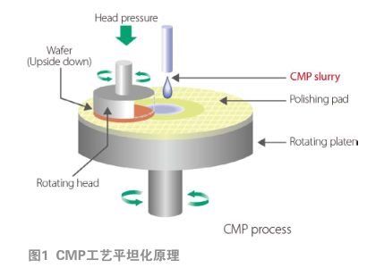
The planarization principle of CMP process is to use mechanical force to act on the surface of the wafer, and at the same time, the chemical substances in the polishing solution react with the surface materials of the wafer to increase its polishing rate (as shown in Figure 1). The equipment and consumables used in CMP technology include: polishing machine, polishing slurry, polishing pad, post-CMP cleaning equipment, polishing endpoint detection and process control equipment, waste treatment and detection equipment, etc. The difficulty of CMP technology is to mix dry and wet, and to find a good balance between chemistry and machinery.
The two most important components in CMP process are polishing liquid and polishing pad. Both polishing liquid and polishing pad are consumables, and the service life of polishing pad is usually 45~75 hours. Polishing solution is divided into acidic polishing solution and alkaline polishing solution, which is an ivory colloid with evenly dispersed colloidal particles, and mainly plays the role of polishing, lubrication and cooling. Taking alkaline SiO _ 2 polishing solution as an example, its components mainly include abrasives (SiO _ 2 colloidal particles), alkali, deionized water, surfactants, oxidants and stabilizers. Polishing pad is a kind of porous material with certain elasticity, which is generally polyurethane. Its main function is to store and transport polishing liquid, provide certain pressure on the silicon wafer and mechanically rub its surface.
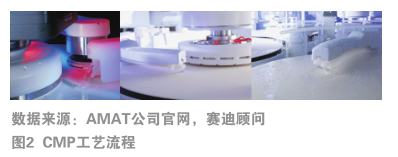
In the CMP process, firstly, the polishing liquid is filled in the gap of the polishing pad, and the wafer is driven by the polishing head to rotate at high speed, which reacts with the polishing pad and the polishing particles in the polishing liquid, and other parameters such as the downward pressure of the polishing head need to be controlled. CMP equipment is mainly divided into two parts, namely, polishing part and cleaning part. The polishing part consists of four parts, namely, three polishing turntables and a wafer loading and unloading module. The cleaning part is responsible for cleaning and spin-drying the wafer to realize "dry in and dry out" (as shown in Figure 2).
1.3 CMP polishing process technical indicators
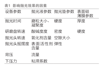
The main detection parameters of CMP include grinding rate, grinding uniformity and defect amount (as shown in Table 1). The grinding rate refers to the total amount of material on the wafer surface ground per unit time. Grinding uniformity can be divided into intra-wafer grinding uniformity and inter-wafer grinding uniformity. The grinding uniformity in a wafer refers to the ratio of the standard variance of the grinding rate of a wafer to the grinding rate; The grinding uniformity between wafers is used to indicate the consistency of grinding rates of different wafers under the same conditions. For CMP, the main defects include surface particles, surface scratches and abrasive residues, which will directly affect the yield of products. The semiconductor industry also has a corresponding "hidden rule" for CMP process, that is, the material loss of the device after CMP process is less than 10% of the thickness of the whole device. That is to say, not only must the material be effectively removed, but also the removal rate and final effect can be accurately controlled. With the shrinking of device feature size, the influence of defects on process control and final yield is more and more obvious, and reducing defects is the core technical requirement of CMP process.
1.4 market price of CMP polishing equipment
CMP is a kind of equipment which integrates many advanced technologies such as mechanics, fluid mechanics, material chemistry, fine machining, control software, etc. It is one of the more complicated and difficult equipments in various integrated circuit production equipment. With the increase of wafer diameter and process complexity, the equipment price of CMP is also increasing gradually. Generally speaking, the price of CMP equipment for 200 mm wafers is about USD 3 million, and that for 300 mm wafers is about USD 4 million.
2 CMP equipment supplier profile
At present, the United States and Japan are in a leading position in the field of CMP equipment manufacturing. The main manufacturers are AppliedMaterials (AMAT) in the United States and Ebara in Japan. The main research and development units of domestic CMP equipment are Tianjin Huahai Qingke and the 45th Research Institute of China Electronics Technology Group Corporation, among which Huahai Qingke’s polishing machine has been tried on SMIC production line. In January 2018, Huahai Qingke’s Cu &Si CMP equipment entered Shanghai Huali.
2.1 American applied materials
CMP equipment is still the only applied material in the United States, with a global market share of 71%. In 2003, Applied Materials of the United States stopped the production of 8-inch equipment and focused on 12-inch CMP equipment. Mirra CMP of Applied Materials Company provided high-performance 150 mm and 200 mm planarization solutions for silicon, shallow trench isolation (STI), oxide, polysilicon, tungsten and copper damascene applications. Its high-speed planarization turntable and multi-zone grinding head have low pressure and can achieve excellent uniformity and efficiency. The integrated Mesa cleaner after CMP (chemical mechanical planarization) (also suitable for 150 mm and 200 mm applications) can effectively remove slurry, prevent residue formation and minimize particles and water marks. For the application of copper inlay, 200 mmDesica cleaning and rinsing technology can also be selected, and Marangoni steam dryer can be used to realize fast and effective watermark-free drying. Applied Materials’ Mirra CMP system adopts a complete set of endpoint methods, provides collinear metrology and advanced process control capabilities, ensures excellent process control and repeatability within and between wafers, and is suitable for all planarization applications. Advanced polishing technology (such as Titan Profiler(150 mm) and Titan Contour (200 mm) polishing head products of Applied Materials Company) and multi-turntable configuration,By adjusting the removal rate across the wafer surface and within 3 mm from the wafer edge, the key uniformity index can be met. These advanced functions and other published upgrades provide more processing capacity guarantee for achieving higher productivity and yield.
2.2 Ebara, Japan
Kurihara Corporation, located in Daejeon, Tokyo, Japan, designs and manufactures social infrastructure and industrial machinery and equipment, and is listed on the Tokyo Stock Exchange. It is also the parent company of Elliott Company, which produces compressors and steam turbines in the United States. Its main businesses are geomechanics, environment and precision electronics. Both 200 mm and 300 mm CMP polishing equipment in Tokyo, Japan have high reliability and high productivity. The 10-20 nm CMP equipment for 12-inch wafers owned by Sakurahara can replace American products to some extent.
Ebara’s global R&D teams in Europe and Japan continue to push the most advanced applications to the forefront of industry production and new technology requirements. In addition to the challenges of MEMS/SOI/magnetic media industry, the Qualcomm F-REX series CMP system of Ebara is running the most demanding applications today, such as oxide, ILD, STI, tungsten and copper for IC manufacturing. They have excellent reliability, and their performance exceeds 250 hours MTBF. The F-REX200 and F-REX300SII platforms suitable for wafer diameters of 200 and 300 mm respectively provide the most advanced design and performance to meet the most advanced device manufacturing requirements. They provide user-oriented system configurations designed to achieve maximum throughput and all drying/drying wafer handling functions. The F-REX200 tool represents the latest CMP technology for 200 mm wafers (150 mm is also available). It adopts EB original patented dry-in-dry-out wafer processing technology. The cleaning module is integrated into the CMP tool, so that the dry wafer is transported to the subsequent process. The F-REX200 system is equipped with two platens, each with one head and four cleaning stations. Four SMIF compatible loading ports can be selected to communicate with CIM host. Other options include endpoint pointing, polishing plate and online metering.
2.3 Huahai Qingke
Since 2000, Professor Lu Xinchun, an academician of Tsinghua University Mechanical Department and a "Changjiang Scholar", has led the research team to engage in polishing technology research, and has made outstanding achievements in the research fields of polishing technology and polishing equipment. In 2012, Tsinghua University successfully developed the first domestic 12-inch CMP equipment with independent intellectual property rights. In March 2013, Tsinghua Holdings and Tianjin established Huahai Zero2IPO to promote the industrialization of this scientific and technological achievement. In 2014, through the transformation of Tsinghua University’s scientific and technological achievements, Hua Haiqing made the first domestic 12-inch "dry in and dry out" CMP commercial model-—Universal-300. In 2015, the machine entered SMIC’s Beijing factory, and passed the SMIC examination and achieved sales in 2016. This fills the blank of CMP equipment technology in the field of integrated circuit manufacturing in China and breaks the foreign monopoly. As of April 2019, the machine has processed more than 60,000 silicon wafers. In February 2017, Huahai Zero2IPO’s second CMP process equipment entered SMIC’s Beijing plant, and it took only 78 days to complete the installation and debugging, and produced more than 100 wafers, creating the highest efficiency of the first domestic core process equipment in the integrated circuit production line, and won the "Outstanding Achievement Award" awarded by SMIC. On January 18, 2018, following the successful completion of the large-scale production of IMD/ILD/STI process products in SMIC, Cu&of Huahai Zero2IPO, a member of Tsinghua Holdings.Si CMP equipment enters Shanghai huali. This is the first time that the domestic CMP machine has entered Shanghai Huali, and it also marks that the first domestic 12-inch copper process CMP equipment has officially entered the integrated circuit production line.
2.4 CLP 45
On the morning of November 21st, 2017, the first domestic 200 mm CMP commercial machine developed by Electrical Equipment 45 passed the rigorous ten thousand-piece marathon test, and was sent to SMIC (Tianjin) for online verification. This means that the equipment in the 45 th Institute of Electrical Equipment has been recognized by users, and the products have moved from the low-end to the high-end. It also marks that the electrical equipment has taken an important step towards realizing the independent control of the core equipment of integrated circuits and shouldering the responsibility of being a big country and a heavy weapon. Hangzhou Zhongde is a newly established company, which was founded by CMP technical experts from 45 Institute of CLP.
2.5 Shengmei Semiconductor
The CMP equipment of Shengmei Semiconductor is mainly used for the 65~45 nm copper interconnection process of back-end packaging. Shengmei has mastered the stress-free polishing technology of wafers, and the prototype using this technology has been purchased by Intel and American LSI Logic Company. At "SEMICON China2019" in Shanghai in March 2019, Shengmei Semiconductor once again released advanced packaging copper throwing equipment, and the newly launched packaging copper throwing equipment was developed for artificial intelligence (AI) chip packaging process. Different from traditional chips, AI chips have more pins, which requires brand-new three-dimensional packaging technology and packaging equipment, and the polishing process requires high-cost polishing powder. According to the requirements of 2.5D packaging technology, this polishing equipment of Shengmei Semiconductor adopts wet electropolishing technology, which not only reduces the consumption of polishing powder (CMP) by about 90%, but also can recover the copper in the polishing solution. Because the chemical solution of electropolishing can be reused, it can save more than 80% of the consumables.
3 CMP equipment investment points
The CMP equipment market is a highly monopolized market, and its market share is mainly concentrated in two giants, American Applied Materials and Japan’s Ebara, which account for 98% of the global CMP equipment market share. Among them, American applied materials is the only one, with a market share as high as 71% in 2018, and the second-ranked Japanese Ebara only accounts for 27% [1]. At present, domestic CMP equipment is mainly low-end products, and 12-inch high-end CMP equipment is mainly in the product verification stage. Although the shipment volume is small, compared with other semiconductor equipment, domestic CMP equipment has made great achievements. The 12-inch CMP equipment independently developed by Huahai Qingke and CLP 45 has filled the gap in China’s CMP equipment market and made important contributions to the domestic substitution of semiconductor equipment in China.
3.1 positive
From the perspective of market prospect, on the one hand, in 2018, the market scale of semiconductor equipment in China increased by nearly 60%, accounting for 20% of the global market share. According to SEMI’s prediction, 62 new semiconductor production lines will be built in the world from 2017 to 2020, among which 26 new production lines will be in Chinese mainland, accounting for 42%, which will bring huge market space for semiconductor equipment. On the other hand, with the rise of new energy vehicles, 5G communication and Internet of Things applications, the demand for MOSFET power devices, power management chips, 5G radio frequency chips, Internet of Things chips, MEMS devices and compound semiconductor devices is very strong, and most of these chips are produced on 200 mm production lines. The global integrated circuit industry is seriously short of capacity and equipment in 200 mm wafer factories, and wafer manufacturers have been seeking to expand 200 mm manufacturing capacity. However, at present, international leading enterprises have basically stopped production of 200 mm equipment, and the price of second-hand 200 mm equipment is also rising, so the market space of 200 mm equipment is huge. Domestic CMP equipment manufacturers have relatively mature 200 mm-inch equipment technology. Domestic equipment manufacturers can seize the excellent situation of the rapid development of integrated circuit industry, rely on industrial policy guidance, seize opportunities and seize the market, and rely on product price advantages to gradually occupy the market space of international manufacturers in individual products or sub-sectors, so as to become bigger and stronger, achieve leap-forward development, and make positive contributions to China’s extremely large-scale integrated circuit manufacturing.
3.2 risks
The relative backwardness of the domestic semiconductor industry has led to the late start of the semiconductor equipment industry, especially in the key equipment field, which is still decades behind the overseas giants. Limited by technology, capital and talents, the domestic semiconductor equipment has a weak foundation, and the industry as a whole shows the characteristics of small enterprise scale, low technical level and scattered industrial layout. However, the development of international semiconductor equipment is relatively mature, and CMP equipment is characterized by a high degree of monopoly. Under the existing competitive pattern, it will inevitably take a lot of time and energy for domestic equipment to start all over again through R&D investment. The products will also compete with overseas giants in the downstream application and promotion process, and downstream manufacturers will also consider the cost factor for substitution. Whether or not to open the downstream market is the key factor for the profit and survival of enterprises.
references
[1] Li Dan. Chemical Mechanical Polishing (CMP) Equipment Market Overview. Electronic Products World, 2019(5):11-13
Brief introduction of the author
Li Dan, Ph.D., intermediate engineer, research interests: integrated circuit materials and equipment, compound semiconductors, artificial intelligence chips.
This article comes from page 31, issue 6, 2019 of the scientific and technological journal Electronic Products World. You are welcome to quote it when writing your paper, and indicate the source.